文章专利

- 地址: 江苏省苏州市苏州工业园区若水路398号
- 邮箱: tzhang2009@sinano.ac.cn
- 电话: 86-512-62872706
- 传真: 0512-62603079
- 网址: http://nanosensor.sinano.ac.cn

“Top-down” and “bottom-up” strategies for wafer-scaled miniaturized gas sensors design and fabrication. “Top-down” and “bottom-up” strategies for wafer-scaled miniaturized gas sensors design and fabrication. . Microsystems & Nanoengineering (2020) 6:31
Lin Liu, Yingyi Wang, Fuqin Sun, Fuqin Sun, Yanbing Dai, Shuqi Wang, Yuanyuan Bai, Lianhui Li, Tie Li, Ting Zhang* and Sujie Qin*

Abstract:
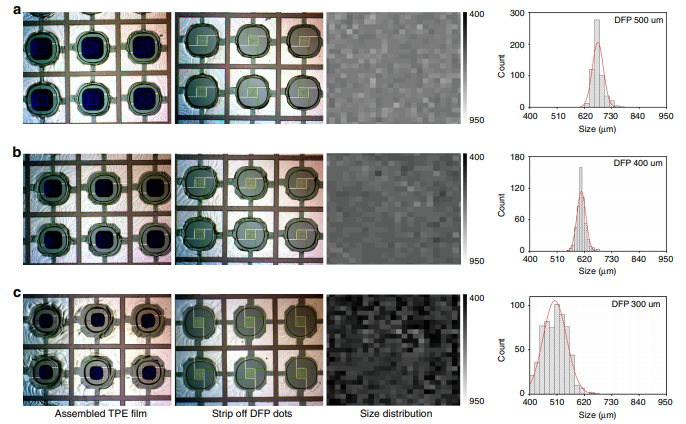
Manufacture of large-scale patterned nanomaterials via top-down techniques, such as printing and slurry coating, have been used for fabrication of miniaturized gas sensors. However, the reproducibility and uniformity of the sensors in wafer-scale fabrication are still a challenge. In this work, a “top-down” and “bottom-up” combined strategy was proposed to manufacture wafer-scaled miniaturized gas sensors with high-throughput by in-situ growth of Ni(OH)2 nanowalls at specific locations. First, the micro-hotplate based sensor chips were fabricated on a two-inch (2”) silicon wafer by micro-electro-mechanical-system (MEMS) fabrication techniques (“top-down” strategy). Then a template-guided controllable de-wetting method was used to assemble a porous thermoplastic elastomer (TPE) thin film with uniform micro-sized holes (relative standard deviation (RSD) of the size of micro-holes <3.5 %, n > 300), which serves as the patterned mask for in-situ growing Ni(OH)2 nanowalls at the micro-hole areas (“bottom-up” strategy). The obtained gas microsensors based on this strategy showed great reproducibility of electric properties (RSD < 0.8%, n = 8) and sensing response toward real-time H2S detection (RSD < 3.5%, n = 8).
Full Article:https://www.nature.com/articles/s41378-020-0144-4
